E-mail
Jiaxing AOSITE Photonics Technology Co.,Ltd.
sic wafer
sic wafer
silicon carbide wafer
sic epi wafer

OST Photonics SiC Wafers

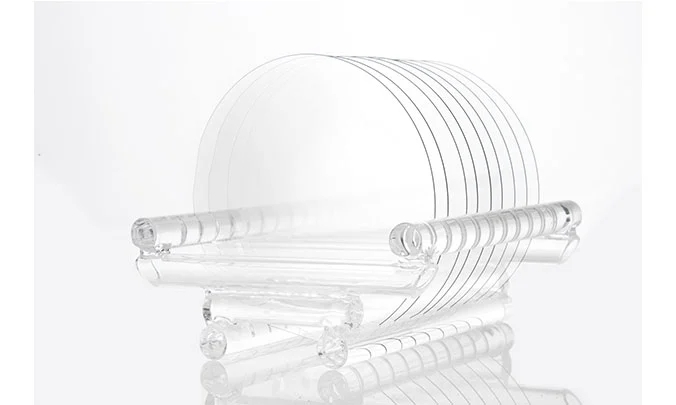
OST Photonics offer 4” and 6” SiC wafers for semiconductor industry. There are two conduct types of SiC materials for you to choose from: N-type SiC (Nitrogen doped) and high purity semi-insulating SiC (undoped). High purity semi-insulating SiC wafers is mainly used in 5G communication applications. It has the advantages of improving the radio frequency range, ultra-long distance recognition, anti-interference, high-speed and large-capacity information transmission, and is regarded as the most ideal material for making microwave power devices. N-type SiC wafer is mainly used in new energy vehicles, high voltage transmission and transformation stations, white goods, high-speed trains, motors, photovoltaic inverter, pulse power supply and other fields, it has the advantages of reducing equipment energy loss, improving equipment reliability, reducing equipment volume, improving equipment performance and so on, it has irreplaceable advantages in the production of power electronic devices. In addition, SiC ingots and customized SiC substrates are also available upon requests.


Application of SiC Wafers


  • 5G Wireless Communication

  • Microwave power device

  • New energy automobile

  • Pulsed power supply

  • Photovoltaic inverter


Advantages of SiC Wafers


  • Large band gap (about 3 times of Si)

  • High critical field strength (about 10 times of Si)

  • High thermal conductivity (about 3 times of Si)


Ability of SiC Wafers


  • Orientation:<0001>,<0001>off 4º

  • Dimension: 4”, 6”, 20x20mm, 15x15mm, 10x10mm, 5x5mm etc.

  • Thickness: 350 μm, 500 μm, 330 μm etc.

  • Available items: wafers, substrates, blanks, ingots and customized products


Product Parameters of 4 Inch High Purity Semi-insulating SiC Wafers


No.ItemsUnitProductionResearchDummy
1 Crystal Parameters
1.1 Polytype
4H4H4H
1.2 Surface orientation onFaxis
<0001><0001><0001>
1.3 Surface orientation off-axis
0±0.2°0±0.2°0±02
1.4 (0004)(FWHM)arcsec≤45arcsec≤60arcsec≤100arcsec
2 Electrical Parameters
2.1 Type
HPSIHPSIHPSI
2.2 Resistivityohm-cm≥1E9ohm-cm100%area>1E5ohm-cm70%area>1E5ohm-cm
3 Mechanical Parameters
3.1 Diametermm99.5~100mm99.5~100mm995~100mm
3.2 Thicknessμm500±25μm500±25μm500±25um
3.3 Primary flat orientation
[1-100]±5°[1-100]±5°[1-100]±5°
3.4 Primary flat lengthmm32.5±1.5mm32.5±1.5mm32.5±1.5mm
3.5 Secondary flat position
90±5°
90°CW from primary flat ±5°,silicon
face up
90±5°
90°CW from primary flat ±5°,silicon
face up
90±5
90°CW from primary flat ±5°,silicon
face up
3.6 Secondary flat lengthmm18±1.5mm18±1.5mm18±1.5mm
3.7 TTVμm≤5μm≤10μm≤20μm
3.8 LTVμm≤2μm(5mm*5mm)≤5μm(5mm*5mm)NA
3.9 Bowμm-15μm~15μm-35μm~35μm-45μm~45μm
3.10 Warpμm≤20μm≤45μm≤50μm
3.11 (AFM)Front (Si-face)RoughrnmRa≤0.2nm(5μm*5μm)Ra≤0.2nm(5μm*5μm)Ra≤0.2nm(5μm*5μm)
4 Structure
4.1 Micropipe Densityea/cm2≤lea/cm2≤5ea/cm2≤10ea/cm²
4.2 Carbon Densityea/cm2≤lea/cm²NANA
4.3 Hexagonal void
NoneNANA
4.4 Metal impuritiesatoms/cm2≤5E12atoms/cm2≤5E12atoms/cm2NA


5 Front Quality
5.1 Front
SiSiSi
5.2 Surface Finish
Si CMP Si-face CMPSi CMP Si-face CMPSi CMP Si-face CMP
5.3 Partidesea/wafer≤60(size≥0.3μm)NANA
5.4 Scratchesea/mm≤2,≤Diameter
(Cumulative Length)
≤2*Diameter (Cumulative
Length)
NA
5.5 Orange
peel/pits/stains/striations/cracks/contamination
mmNoneNoneNA
5.6 chips/indents/fracture/hex plates
NoneNoneNone
5.7 Polytype areas
None≤20%(Cumulative area)≤30%(Cumulative area)
5.8 Front laser marking
NoneNoneNone
6 Back Quality
6.1 Back Finish
C CMP C-face CMPC CMP C-face CMPC面CMP C-face CMP
6.2 Scratchesea/mm≤5,≤2*Diameter
(Cumulative Length)
NANA
6.3 Back defects (edge chips/indents)
NoneNoneNone
6.4 Back roughnessnmRa≤0.2nm(5μm*5μm)Ra≤0.2nm(5μm*5μm)Ra≤0.2nm(5μm*5μm)
6.5 Back laser marking
1mm (from top edge)1mm(from top edge)1mm (from top edge)
7 Edge
7.1 Edge
ChamferChamferChamfer
8 Packaging
8.1 Packaging
The inner bag is filled with nitrogen and the outer bag is vacuumed.The inner bag is filled with nitrogen and the outer bag is vacuumed.The inner bag is filled with nitrogen and the outer bag is vacuumed.
8.2 Packaging
Multi-wafer cassette,epi-ready.Multi-wafer cassette,epi-ready.Multi-wafer assette,epi-ready.


Product parameters of 6 inch high purity semi-insulating SiC wafers


No.ItemsUnitProductionResearchDummy
1 Boule Parameters
1.1 Polytype
4H4H4H
1.2 Surface orientation on-axis
<0001><0001><0001>
1.3 Surface orientation off-axiso0±0.25°0±0.2°0±0.2°
1.4 ( 0 0 0 4 )  ( F W H M )arcsec≤45arcsec≤60arcsec≤100arcsec
2 Electrical Parameters
2.1 Type
HPS I O RHPSIHPSI
2.2 Resistivityohm ·cm≥1E8ohm ·cm100%area>1E5ohm ·cm70%area>1E5ohm-cm
3 Mechanical Parameters
3.1 Diametermm150±0.2mm150±0.2mm99.5~100mm
3.2 Thicknessμm500±25um500±25μm500±25um
3.3 Notch Notch orientationo[1-100]±5°[1-100]±5°[1-100]±5°
3.4 Notch Notch Depthmm1~1.25mm1~1.25mm1~1.25mm
3.6 L TVμm≤3μm(5mm*5mm)≤5μm(5mm*5mm)≤10μm(5mm*5mm)
3.5 T TVμm≤5μm≤10μm≤15μm
3.7 Bowμm-25μm~25μm-35μm~35μm-45μm~45μm
3.8 Warpμm≤35μm≤45μm≤55μm
3.9 Front RoughnessnmRa≤0.2nm(5μm*5μm)Ra≤0.2nm(5μm*5μm)Ra≤0.2nm(5μm*5μm)
4 Structure
4.1 Micropipe densityea/cm≤1  ea/cm²≤10ea/cm²≤15ea/cm²
4.2 Carbon inclusions densityea/cm²≤1  ea/cm²NANA
4.3 Hexagonal void
NoneNANA
4.4 Metal impuritiesatoms/cm²≤5E12atoms/cm≤5E12atoms/cm2NA
5 Front Quality
5.1 Front
SiSiSi
5.2 Surface Finish
Si CMP Si-face CMPSi CMP Si-face CMPSi CMP Si-face CMP
5.3 Particlesea/wafer≤60(尺寸size≥0.3μm)NANA
5.4 Scrachesea/mm≤5,≤Diameter
(Cumulative Length)
≤2*Diameter
(Cumulative Length)
NA
5.5 Orange peel/pits/stains/striations/cracks/contamination
NoneNoneNA
5.6 Edge chips/indents/fracture
NoneNoneNone
5.7 Polytype areas
None≤20%(Cumulative
area)
≤30%(Cumulative
area)
5.8 Front laser marking
NoneNoneNone
6 Back Quality
6.1 Back finish
C CMP C-face CMPC CMP C-face CMPC CMP C-face CMP
6.2 Scrachsea/mm≤5,≤2*Diameter
(Cumulative Length)
NANA
6.3 Back defects (edge
chips/indents)

--
NoneNoneNone
6.4 Back roughnessnmRa≤0.2nm(5μm*5μm)Ra≤0.2nm(5μm*5μm)Ra≤0.2nm(5μm*5μm)
6.5 Back laser marking--SEMISEMISEMI
7 Edge
7.1 Edge
Chamfer倒角处理Chamfer倒角处理Chamfer
8 Packaging
8.1 Packaging
The inner bag is filled with nitrogen and the outer bag is vacuumedThe inner bag is filled with nitrogen and the outer bag is vacuumedThe inner bag is filled with nitrogen and the outer bag is vacuumed.
8.2 Packaging
Multi-wafer cassette,epi-ready.Multi-wafer cassette,epi-ready.Multi-wafer cassette,epi-ready.
Notes:"NA"means no request.Items not metioned may refer to SEMI-STD.


Product parameters of 4 inch N-type SiC wafers


No.ItemsUnitProductionResearchDummy
1 Boule Parameters
1.1 Polytype
4H4H4H
1.2 Surface orientation error
<11-20>4±0.15<11-20>4±0.15<11-20>4±0.15
2 Electrical Parameters

2.1 Dopant
n-type Nitrogenn-type Nitrogenn-type Nitrogen
2.2 Resistivityohm ·cm0.015~0.0250.015~0.0250.015~0.025
3 Mechanical Parameters
3.1 Diametermm99.5~100mm99.5~100mm99.5~100mm
3.2 Thicknessμm350±25350±25350±25
3.3 Primary flat orientationo[1-100]±5[1-100]±5[1-100]±5
3.4 Primary flat lengthmm32.5±1.532.5±1.532.5±1.5
3.5 Secondary flat
90±5°90±5°90±5°
3.6 Secondary flat lengthmm18±1.5mm18±1.5mm18±1.5mm
3.8 LTVμm≤2(5mm*5mm)≤5(5mm*5mm)NA
3.7 TTVμm≤5≤10≤20
3.9 Bowμm-15~15-35~35-45~45
3.10 Warpμm≤20≤45≤50
3.11 (AFM)Front (Si-face)
Roughness
nmRa≤0.2(5μm*5μm)Ra≤0.2(5μm*5μm)Ra≤0.2(5μm*5μm)
4 Structure
4.1 Micropipe densityea/cm²≤1≤5≤10
4.2 Metal impuritiesatoms/cm≤5E10≤5E10NA
4.3 BPDea/cm²≤2000≤3000NA
4.4 TSDea/cm≤500≤1000NA
5 Front Quality
5.1 Front
SiSiSi
5.2 Surface Finish
Si面CMP Si-face CMPSi面CMP Si-face CMPSi面CMP Si-face CMP
5.3 Particlesea/wafer≤60(尺寸size≥0.3μm)NANA
5.4 Scratchsea/wafer≤2,Total Length≤Diameter累计长度≤2*DiameterNA
5.5 Orange peel/pits/cracks/contamination/stains/striations
NoneNoneNA
5.6 Edge chips/indents/fracture
NoneNoneNA
5.7 Polytype areas
None≤20%≤30%
5.7 Front laser marking
NoneNoneNone
6 Back Quality
6.1 Back finish
C-face polishedC-face polishedC-face polished
6.2 Scrachesea/mm≤5,Total Length≤2*DiameterNANA
6.3 Back defects (edge
chips/indents)

NoneNoneNone
6.4 Back roughnessnmRa≤0.2(5μm*5μm)Ra≤0.2(5μm*5μm)Ra≤0.2(5μm*5μm)
6.5 Back laser marking
1mm (from top edge)1mm (from top edge)1mm (from top edge)
7 Edge
7.1 Edge
ChamferChamferChamfer
8 Packaging
8.1 Packaging
The inner bag is filled with
nitrogen and the outer bag is vacuumed.
The inner bag is filled with
nitrogen and the outer bag is vacuumed.
The inner bag is filled with nitrogen and the outer bag is vacuumed.
8.2 Packaging
Multi-wafer cassette,epi-ready.Multi-wafer cassette,epi-ready.Multi-wafer cassette,epi-ready.
Notes:"NA"means no request.Items not metioned may refer to SEMI-STD.


Product parameters of 6 inch N-type SiC wafers:


No.ItemsUnitProductionResearchDummy
1 Boule Parameters
1.1 Polytype
4H4H4H
1.2 Surface orientation error
<11-20>4±0.15<11-20>4±0.15<11-20>4±0.15
2 Electrical Parameters

2.1 Dopant
n-type Nitrogenn-type Nitrogenn-type Nitrogen
2.2 Resistivityohm-cm0.015~0.0250.015~0.0250.015~0.025
3 Mechanical Parameters
3.1 Diametermm150.0±0.2150.0±0.2150.0±0.2
3.2 Thicknessμm350±25350±25350±25
3.3 Primary flat orientation
[1-100]±5[1-100]±5[1-100]±5
3.4 Primary flat lengthmm47.5±1.547.5±1.547.5±1.5
3.5 Secondary flatmmNoneNoneNone
3.6 LTVμm≤3(5mm*5mm)≤5(5mm*5mm)≤10(5mm*5mm)
3.7 TTVμm≤5≤10≤15
3.8 Bowμm-25~25-35~35-45~45
3.9 Warpμm≤35≤45≤55
3.10 (AFM)Front (Si-face)RoughnessnmRa≤0.2(5μm*5μm)Ra≤0.2(5μm*5μm)Ra≤0.2(5μm*5μm)
4 Structure
4.1 Micropipe densityea/cm²<1<10<15
4.2 Metal impuritiesatoms/cm≤5E10≤5E10NA
4.3 BPDea/cm≤2000≤3000NA
4.4 TSDea/cm²≤500≤1000NA
5 Front Quality
5.1 Front
SiSiSi
5.2 Surface Finish
CMP Si-face CMPCMP Si-face CMPCMP Si-face CMP
5.3 Particlesea/wafer≤60(尺寸size≥0.3μm)NANA
5.4 Scratchsea/wafer≤5,Total Length≤DiameterTotal Length≤2*DiameterNA
5.5 Orange peel/pits/cracks/contamination/stains/striations
NoneNoneNA
5.6 Edge chips/indents/fracture
NoneNoneNone
5.7 Polytype areas
None≤20%≤30%
5.8 Front laser marking
NoneNoneNone
6 Back Quality
6.1 Back finish
C-face polishedC-face polishedC-face polished
6.2 Scrachesea/mm≤5,Total Length≤2*DiameterNANA
6.3 Back defects (edge chips/indents)
NoneNoneNone
6.4 Back roughnessnmRa≤0.2(5μm*5μm)Ra≤0.2(5μm*5μm)Ra≤0.2(5μm*5μm)
6.5 Back laser marking
1mm (from top edge)1mm (from top edge)1mm (from top edge)
7 Edge
7.1 Edge
ChamferChamferChamfer
8 Packaging
8.1 Packaging
The inner bag is filled with nitrogen and the outer bag is vacuumed.The inner bag is filled with nitrogen and the outer bag is vacuumed.The inner bag is filled with nitrogen and the outer bag is vacuumed.
8.2 Packaging
Multi-wafer cassette,epi-ready.Multi-wafer cassette,epi-ready.Multi-wafer cassette,epi-ready.
Notes:"NA"means no request.Items not metioned may refer to SEMI-STD.


Product parameters of 4 inch N-type SiC ingots:


No.ItemsUnitProductionResearchDummyDate
1. Ingot Parameters
1.1 Polytype
4H*
1.2 Dopant
n-type Nitrogen*
1.3 Resistivityohm ·cm0.015~0.025*
1.4 Diametermm100.25±0.25#
1.5 Thicknessmm≥10(Figure 2)#
1.6 Surface orientation error4°toward<11-20>±0.2°(Figure 1)#
1.7 Primary flat orientationo[1-100]±5.0(Figure 4)*
1.8 Primary flat lengthmm32.5±1.5(Figure 3)#
1.9 Secondary flat90.0°CW from Primary±5.0°,silicon face up(Figure 4)*
1.10 Secondary flat lengthmm18±1.5(Figure 3)#
1.11 Micropipe densityea/cm²≤0.5≤5≤10*
1.12 BPDea/cm²≤2000≤3000
*
1.13 TSDea/cm²≤500≤1000
*
1.14 Edge Cracksea≤3,≤1mm/ea≤5,≤1mm/ea≤5,≤3mm/ea#
1.15 Polytype areas
--
None≤3%area≤5%area*
1.16 Edge indents
ea
≤3,≤1mm width and depth≤5,≤1mm width and depth≤5,≤2mm width and depth#
2. Packaging
2.1 Label
C-face(Figure 5)*
2.2 Packaging
--
unit-ingot cassette、vacuum packaging*
Notes:*means guarantee value.#means actually measured value that can be provided.


Product parameters of 6 inch N-type SiC ingots:


No.ItemsUnitProductionResearchDummyDate
1. Ingot Parameters
1.1 Polytype
4H*
1.2 Dopant
n-type Nitrogen*
1.3 Resistivityohm ·cm0.015~0.025*
1.4 Diametermm150.25±0.25#
1.5 Thicknessmm≥10(Figure 2)#
1.6 Surface orientation error4°toward<11-20>±0.2°(Figure 1)#
1.7 Primary flat orientationo[1-100]±5.0(Figure 4)*
1.8 Primary flat lengthmm47.5±1.5(Figure 3)#
1.9 Micropipe densityea/cm²≤0.5≤5≤10*
1.10 BPDea/cm²≤2000≤3000
-
*
1.11 TSDea/cm²≤500≤1000
--
*
1.12 Edge Cracksea≤3,≤1mm/ea≤5,≤1mm/ea≤5,≤3mm/ea#
1.13 Polytype areas
None≤3%area≤5%area*
1.14 Edge indentsea≤3,≤1mm width and depth≤5,≤1mm width and depth≤5,≤2mm width and depth#
2. Packaging
2.1 Label
C-face(Figure 5)*
2.2 Packaging
unit-ingot cassette、vacuum packaging*
Notes:*means guarantee value.#means actually measured value that can be provided.


Contact Us
Welcome your presence, you can send us an email, we will get in touch with you within 24 hours.
Head Office: No. 66, 8 Group, Chengbei Village, Yanguan Town, Jiaxing 314411, China;

Hangzhou Branch: Room 1012, Chunhua Bussiness Center, No. 159, Hangbo Street, Shangcheng District, Hangzhou 310009, Zhejiang, China
Head Office: No. 66, 8 Group, Chengbei Village, Yanguan Town, Jiaxing 314411, China;

Hangzhou Branch: Room 1012, Chunhua Bussiness Center, No. 159, Hangbo Street, Shangcheng District, Hangzhou 310009, Zhejiang, China
sales@ostphotonics.com; info@ostphotonics.com +86-0571-86780460